■ Electron transport of quantum dot polymers by combining field effect transistor technology with quantum dynamics formalism ■□ Electron transport of quantum dot polymers by combining field effect transistor technology with quantum dynamics formalism
In theory, to study mechanism on the electron transport of quantum dot polymer modeling, a field effect transistor (field-effect transistor) is built in the channel layer as shown below, and (a), performed by combining reduced density matrix formalism and theoretical system. 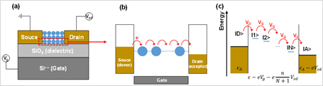
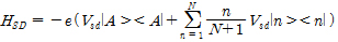
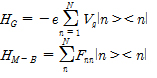
The one-dimensional case to consider the electron transport in the quantum dot array (b, c). The Hamiltonian of system is configured as follows: 
Herein, HQ, HSD, HG, HB, HQ-B are each quantum dot (HQ), source-drain (HSD), gate (HG), ambient thermal (HB), the interaction of quantum dot-bath (HQ-B) Hamiltonian. 

By using Born- Markov approximation, the reduced density matrix ρ can be obtained by Redfield equation: 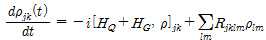
In this scheme, the steady-state rate is naturally defined by 
From the one-dimensional structure above, we extend it in a three-dimensional structure of the actual quantum dot. Hamiltonian of three-dimensional model structure is to be modified, and in particular, to reflect the gradient of the position of the source-drain and gate voltages must each be: 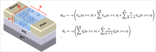
A study on electron transport of quantum dot polymers by combining field effect transistor technology with quantum dynamics formalism
□ Field Effect Transistor Technology Indium (III) Oxide Semiconductors Nanocrystal for TFTs
To employ indium oxide colloidal nanocrystals (In2O3 NCs) in electronic devices, it is necessary to establish efficient electronic communication between individual nanocrystals. The conduction in nanocrystal solids involves charge transfer between individual nanocrystals. Surface ligands with long hydrocarbon chains, used for nanocrystal synthesis, form highly insulating interparticle barriers and result in a very weak exchange coupling between the nanocrystals. Charge transport can be improved by replacing bulky ligands with smaller capping molecules such as pyridine, n-butylamine, etc. so that the electronic coupling between adjacent nanocrystals increases. Our group has proposed entirely new chemical approach for designing electronic materials from colloidal nanocrystals. The shorter organic ligands greatly facilitate electronic coupling between the NCs. For example, thin films made from 2AP-capped In2O3 NCs exhibited a high electron mobility of μ ≈ 9.5 cm2/V·s, an on-off current ratio of about >107, and a subthreshold swing of 2.34 V/decade. As the length of the ligand length decreased, the electron mobility increased exponentially 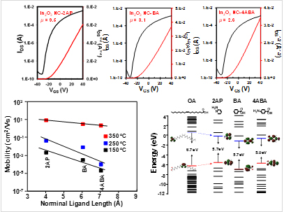
□ Newly application of hybrid materials consisting of π-conjugated polymers (or oligomers) and semiconductor nanocrystals.
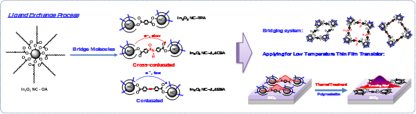
Charge transfer from the nanocrystal aggregates (NC assembly) is expressed through the hopping mechanism. In hopping, transfer integral is determined by charge carrier mobility, which can be improved through the transfer integral adjustment. By hybrid with π-conjugated molecule forms nanocrystal-molecule hybrid polymer (an extension of wavefunction), this new material will be a promising candidate for high performance thin film transistor oxide semiconductor NCs processed at low temperature.
□ Electron transport mechanism in In2O3 NCs Solid
The temperature dependence of the mobility takes the general form: 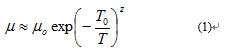
Where µ is the mobility pre-exponential factor, T0 is a fitting parameter with units of Kelvin, and z is temperature coefficient that describes the power of the temperature dependence. z is usually seen to be positive with values around 0.25 for Mott variable-range hopping (M-VRH) 3-demensional transport, 0.33 for Mott variable-range hopping (M-VRH) for 2-demensional transport, 0.5 for Efros-Shklovskii variable-range hopping (ES-VRH) or 1.0 for Arrhenius-like nearest neighbor hopping (NNH). For this reason, a negative z is often taken as an unambiguous sign for the occurrence of band-like transport.
□ Hopping Mechanism in In2O3 NCs Solid.
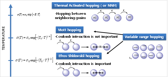
Electron transport in the In2O3 NC TFTs will follow hopping transport equation (1) can be derived from a more general expression for hopping between disordered states: 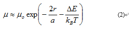
Where µ is the temperature independent pre-exponential factor, r is the spatial distance between states that are involved in hopping (or the hopping distance), a is the localization length of wavefunction of a carrier, ΔE is the energy difference between these states (or activation energy), kB is the Boltzmann constant and T is temperature. At low temperature the essence of VRH can be summarized as below. A hopping electron will always try to find the lowest activation energy ΔE and the shortest hopping distance. However, usually the two conditions cannot be satisfied at the same time. Thus there will be an optimum hopping distance r*, which maximizes the hopping probability. Equation (4) become: 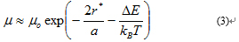
Note that r* is a function of temperature and decreases with increasing temperature Thus, at high temperature (room temperature region), the optimum hopping distance eventually becomes equal to the nearest neighbor distance (d), which is the sum of the particle diameter and interparticle spacing. Physically, the hopping distance cannot be any shorter than the nearest neighbor distance. Hence, the hopping distance above this specific temperature (Tc - crossover temperature), where r* becomes equal to d, is independent of temperature and becomes constant (r*=d=constant). Therefore, above Tc equation (3) reduces to: 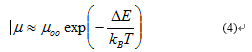
Where µ00 = µ0exp(-2d/a) which is constant. Equation (6) assembles Arrhenius-like T dependence, with activation energy Ea = ΔE and hopping distance is nearest neighbor distance r*=d. Electron transport mechanism in dimethylformamide capped In2O3 NCs (In2O3-DMF NCs). 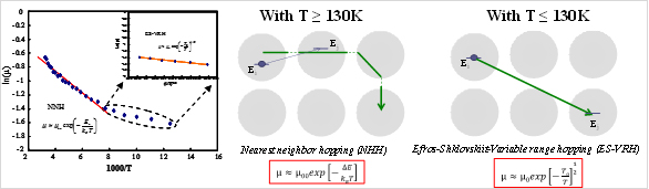
With T ≥ 130K our data fits best with thermally-activated hoping or NNH. With T ≤ 130K our data can fit by Efros-Shklovskii variable-range hopping (ES-VRH). TC = 130 K is crossover temperature from NNH to ES-VRH in our In2O3 NCs thin film Thermally-activated hoping (NNH ) in In2O3-BF4- NCs Solid 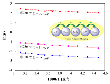
the activation energy (Ea) can be derived according to the slope of Arrhenius plot Ea are 32 meV, 31 meV and 25 meV for In2O3-BF4- NCs thin film annealed at 150 oC, 250 oC and 350 oC, respectively.
□ BaTiO3 Nanocrystal Dielectrics for Thin Film Transistor (TFT)
Our group is trying to develop new dielectrics for low operating voltage of TFTs (Thin-Film Transistors). BaTiO3 nanocrystals are representative examples. These dielectrics are compatible with organic semiconductors, as well as thin films. Furthermore, the resulting BaTiO3 NC/SiO2-based TFTs operate at extremely low voltages and exhibit greater mobility of FETs than analogous TFTs fabricated with conventional SiO2 gate dielectrics owing to the unique BaTiO3 NC combination of high dielectric constant, nanometer thickness, low gate leakage current, and low interface trap state densities. 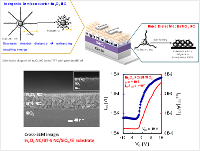
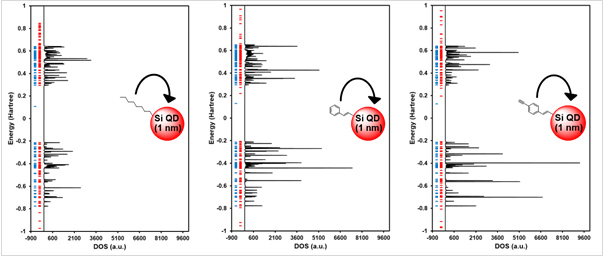
□ Effect of Capping Group on Density of States of Silicon Quantum dot Using Green’s Function Formalism
Using NEGF formalism, our group will build a new theory about interaction between quantum dot and surface molecule. Properties of silicon quantum dots are considerably changed according to the different type of surface molecules which have an effect on the silicon quantum dot system. In this study, we calculate the effect of capping group on DOS for silicon quantum dot system which capping group is octyl, styryl and ethynylstyryl. It is found that, the intensity of density of state is much stronger when there are many conjugation systems in the surface molecule (octyl < styryl < ethynylstyryl). In addition, DOS of silicon quantum dot has a very similar energy state compared with molecular orbital energy of silicon quantum dot. 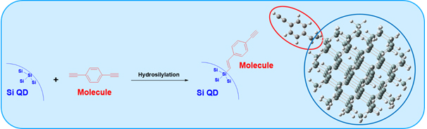
|